The PCB Advantage

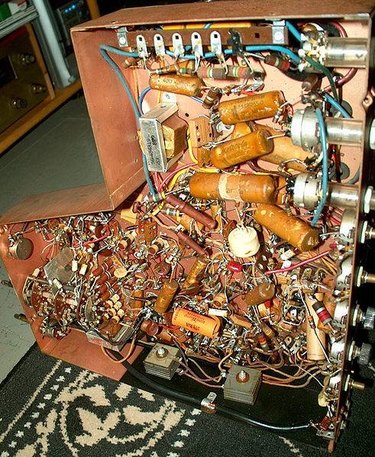
A Printed Circuit Board, or "PCB," has several major advantages compared to older ways of building electronics. In the past, every component inside of an electronic device was connected with large wires and placed anywhere they could fit. As you can see in this picture of a 1948 television, this method was very "messy," and used a large amount of space. PCBs use a different approach. Components are mounted on a non-conductive board and connected with small pathways, called "traces." Because they are usually designed on a computer, printed circuit boards fit many components in a minimum amount of space.
Parts of a PCB
Video of the Day

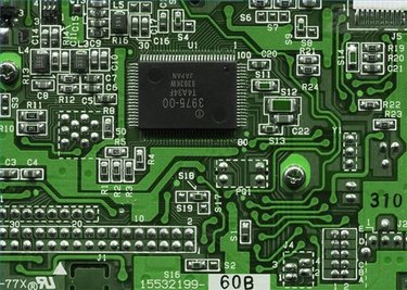
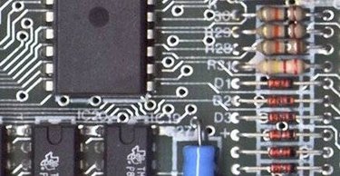
When looking at a printed circuit board, the traces are easily noticeable. These thin lines are conductive and connect all the components in the circuit. They replace the much larger wires used in the past. A PCB also has many tiny holes. These are drilled exactly where each component needs to be placed. For example, if a microchip is part of the circuit and requires eight connections, the same number of holes will be made on the board. This way, parts of the electronic circuit can be mounted completely flush, without long leads or wires. Again, this saves significant space. The final parts added to a PCB are the components themselves. These are the small electrical devices that must be linked for the unit to work. Common components include microchips, diodes, resisters and switches. The components perform the "work" of the circuit, while the printed circuit board provides the connections.
Video of the Day
Creating PCBs

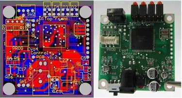
Today, the vast majority of electronic circuits are designed on a computer. This allows electronic engineers to create the perfect arrangement of parts, before making the design permanent. Much like ink on paper, PCBs are literally "printed" when ready. A raw circuit board has two layers, the bottom being non-conductive, and the top being a sheet of metal such as copper. Etch-resistant ink is printed onto the metal layer in the design required. The board is then etched with chemicals. This removes the metal layer, except where the design has been printed. The result: conductive traces remain in the pattern needed for the circuit. Once components are connected to the board with soldering, the PCB is tested and shipped. The entire process is often completely automated, with thousands or millions of the same circuit board being manufactured for use around the world.